Pesquisar este blog

terça-feira, 5 de novembro de 2013

Solder Reliability Tests

With the advent of lead-free it is essential to evaluate several possible alloy combinations and select the most appropriate substitute for lead-based solder. 
In surface mount technology (SMT) lead is widely used in components, solder paste, and board surface finishes, hence eliminating lead would involves changes to the entire assembly process. 
A complete lead-free transition would require careful modification of several process parameters. Any lead-free alloy replacing lead-based solder should qualify with requirements such as low melting point, adequate wetting characteristics, comparable cost, consistent manufacturability (at the component level and the board level), wide availability, acceptable reliability, ease of reworkability and reparability etc [1].
Several possible combinations for lead-free are available in the market. Most commonly used lead-free solder paste is SAC305. Many alloys in this family typically have melting points ranging from 217°C to 222°C. 
Lead-free solder bumps comprises of combinations such as SAC105, SAC305, SAC405, SnAg, etc. Choosing a combination of lead-free solder bump and lead-free solder paste would
dictate the reliability of the assembly.
Today’s hand held devices are subjected to many stresses and hence requiring them to have to reinforce mechanical strength. For superior protection of solder joints against mechanical strains such as shock, drop and vibration, underfill technology should be adopted. 
Underfill technology aims to ensure that area array packages assembled on PCBs can withstand mechanical and thermal shock [2]. In order to prevent the solder joint strain at corner balls it was decided to underfill only the four corners of the package.

thermal_shock_and_drop_test_smta.pdf

Bono Test

Lead free soldering with no clean solder pastes represent nowadays the most common process in electronic assembly. 
A solder paste is usually considered as no-clean if it passes all IPC J-STD-004 corrosion tests: copper mirror, copper panel corrosion test, Surface Insulation Resistance (SIR) and Elecrochemical Migration (ECM). 
Other SIR and ECM tests are described in Bellcore GR-78-CORE and JIS Z3197 standards.
Although SIR and ECM tests are recognized by all standards authorities to evaluate the solder paste residue corrosivity after reflow, a more selective method, the Bono test, has been developed and implemented in some French companies as a qualification criterion. It has been proven that compared to common corrosion tests, the Bono test better differentiates the nature of solder paste residues.

Bono Test Description

This method is based on an existing test which assesses the liquid soldering flux residue corrosivity after wave soldering. 
The test board has been modified to measure the solder paste residue corrosivity from the one used in the SIR and ECM tests. It is composed of 10 electrolytic cells and is made of an FR4 epoxy substrate with a single copper layer, having a very thin anode between two cathodes.
The solder paste is printed on cathodes through a 120µm thickness stencil and reflowed according to the desired profile.

References

1. J. Guinet, X. Lambert and D. Bono, Soldering and Surface Mount Technology, No 16, February 1994

2. Inventec procedure, MO.SB.10029, January 2007

3. IPC-9201, Surface Insulation Resistance Handbook, 1996

4. L. Lach, R. Mellitz, F. Sledd, L. Turbini, J. Schodorf, Developing a Standard Test Method to Indentify Corrosive Soldering Fluxes Residues, International Conference on Solder Fluxes and Pastes 1992

5. IPC-TR-476A, Sixth Working Draft, April 1995

6. IPC J-STD-004B, 2008

7. Bellcore GR-78-Core, 1997

8. JIS Z 3197, 1986 and Z 3284, 1994

9. H. Daniel, M. Leturmy, S. Lazure, T. Vukelic, “Influence of N2 atmosphere on the contamination effects of lead-free  solder paste during reflow soldering process”, APEX 2005

sexta-feira, 13 de setembro de 2013

FMEA

Failure Mode and Effect Analysis

Purpose:

  • Track down and remove special causes of variation.
  • Verify that controls for key and critical product characteristics are addressed in the process.
  • To identify the unacceptable process outputs that can be created at each process step, the causes, the severity and the method of control to prevent or detect the potential unacceptable process outputs.
  • To identify the possible ways in which non-conformities can occur in a manufacturing process, and recommend actions to prevent the nonconformities and/or detect them before the non-conforming parts are shipped to the customer.

Process FMEA Inputs:

  • DFMEA (If available)
  • Customer Returns, Complaints, Corrective Actions
  • Internal NR Data
  • Characteristic Matrix
  • Process Map
  • Final Inspection Reject Data
  • Process Capability Studies (Cpk)
  • MSA Studies

Key Analysis Considerations:

• Characteristic Accountability
• Self QC
• Product Handling
• Administrative Errors
• Assembly Errors
• Part Marking Errors
• F.O.D.
• Packing
• Shipping Damage
• Customer Perception

Brainstorming tools that will assist with developing a process FMEA:

• Ishikawa Diagrams (Fish Bone)
• Five Why’s

quinta-feira, 12 de setembro de 2013

Six Sigma

Six Sigma: “A comprehensive and flexible system for achieving, sustaining and maximizing business success. Six Sigma is uniquely driven by close understanding of customer needs, disciplined use of facts, data, and statistical analysis, and diligent attention to managing, improving, and reinventing business processes.”
Pande, Newman & Cavanagh
The Six Sigma Way

  • A statistical measurement of the performance of a process or a product;
  • A goal that reaches for near perfection in performance;
  • A system of management to achieve lasting business leadership and world-class performance.
Why Six Sigma?
 Eliminate Variability in Products
  •  Nominal Characteristics (Mean or Average)
  •  Spread Between Products (Standard Deviation)
 Is 99% “Good Stuff” Good Enough?
It means...
  •  20,000 Lost Articles of Mail Per Hour
  •  200,000 Wrong Drug Prescriptions Per Year
  •  No Electricity for 7 Hours Per Month
  •  Unsafe Drinking Water 15 Minutes Each Day
  •  2 Short / Long Landings at Most Airports Each Day
IS THIS GOOD ENOUGH ????


quinta-feira, 29 de agosto de 2013

Soldering

Soldering Basics

Posted on 06 November 2012 - http://www.powerguru.org/soldering-basics/


Soldering is the connection of two metallic materials using molten metal or a liquid alloy. The soldered region is heated to the point where the solder melts completely. The solder then has the characteristics of a liquid which spreads over the surface via capillary action. Solder molecules diffuse into the metal surface of the components to be soldered and a thin layer of an alloy is created.
Soldering
Figure 1. Soldering
The pieces of metal are connected after the source of heat is removed and the solder cools down to the point of solidification.
In order for the diffusion process to take place, both metal surfaces must be clean and free of oxides. Fluxing agents are therefore used to clean the surfaces. These fluxing agents are activated once the materials are warmed for soldering. The fluxing agents protect the surfaces from re-oxidation during the soldering process. Most fluxing agents must be removed after soldering since they produce reducing gases and are corrosive. An effective way of achieving void free connection is by applying a vacuum as soon as the solder is liquidized. For industrial production, protective gas can be used to achieve better coverage.

Phase Diagram of Solder Material

Solder is made up of two metals that can mix without leaving voids. The solder is always solid at values below the solidus temperature and liquid at temperature aboves the liquidus temperature. The solder is "pasty" at temperatures that lie within the region between the solidus and liquidus temperatures.
Phase Diagram
Figure 2. Typical phase diagram for solder material
Solder can also be made up of two metals with an eutectic mixture of both metals. For the eutectic composition of the soldering alloy, the solidus and liquidus curves fall alongside each other such that the entire solder melts and solidifies at the eutectic temperature. The eutectic mixture is a fine crystal paste made of pure components of metal A and metal B.
Eutectic system phase diagram
Figure 3. Phase diagram for eutectic system
Solder comes in  two main forms - as preforms and as soldering paste. The soldering paste is a suspension of soldering powder and a liquid. This liquid can either be soluble in water or in some other agent that is used in conjunction with the soldering powder.

Soldering agents

The main components of solder that are normally used in semiconductors are lead (Pb) or tin (Sn). Lead solder that contains a small percentage of tin and/or silver has a melting point of 280°C - 320°C. These solders are usually ductile and have good thermal stability. Tin solder, on the other hand, that contains 1% - 3% silver and/or copper (and sometimes <1% indium) has a melting point of about 225°C. These solders are less ductile and have less thermal stability than lead solder.
The eutectic solder alloy SnPb(37) that contains 63% tin and 37% lead melts at 183°C. A few years ago, this was the standard solder alloy used in electronics due to its low melting point, which served to protect electronic components. However, problems occurred when high temperatures were required. According to EU law RoHS, it is forbidden to use lead in electronic components. An exception has however been made for semiconductor elements.
Wetting is an important criterion for successful soldiering. The wetting angle, the angle between a drop of the liquid solder and the base material (figure 4) is rated as follows:
  • from 0 - 30°: completely/sufficiently wetted
  • from 30 -90°: partly wetted
  • at approximately 180°: not wetted
Solder wetting
Figure 4. Solder wetting and wetting angle

Reflow Soldering

In the reflow soldering process, soldering material is either in the form of a preform or as solder paste. The solder paste is a suspension of soldering powder in a given liquid. This liquid material can either be water soluble or soluble in another solvent. No-clean pastes contain very little fluid and do not have to be cleaned off after the soldering process. No-clean pastes present a compromise between good fluxing properties (wetting) and easy processing. The application of the soldering paste can be done through dispensing or by sieve or screen printing. A solder mask is applied on the base material before the soldering paste is applied in order to prevent the molten solder from overflowing.
Solder mask on a DCB chip
Figure 5. Solder mask on a DCB Mask
Figure 5 above shows a DCB (Direct Copper Bonding) substrate containing 20 individual substrates. The green field and stripes are made of solder mask which is applied in the very first step of the process. This prevents the surface from wetting during the process, ensuring that the chip remains in place throughout the process. This also prevents the solder from being to thin on one chip and overflowing onto the neighbouring chips which would result in too thick of a solder layer on the neighbouring chips.
DCB Card before the soldering process
Figure 6DCB Card before the soldering process
Figure 6 shows a DCB card after the application of the solder by screen printing and the assembling of the chip. A given amount of time must not be surpassed between the assembling of the chip and the soldering process, since the fluid composition required might change due to evaporation. Vapor from the surrounding air can also get into the soldering paste which can result in an explosion like vaporisation rendering the entire card unusable.
DCB Card after the soldering process
Figure 7. DCB Card after the soldering process
Figure 7 shows a DCB after the soldering process. The chips in their correct positions and the solder deposit is molten. Since there is left over soldering paste on the surface, a thorough clean up is required. Aftter the aluminum wire bonding process, the DCB is separated into individual substrates, often by use of lasers. The individual substrates that have defects are marked with a black dot. This damage occurs during the DCB process. These substrates can not be assembled and have to be destroyed.
The heat used in soldering can be derived by several methods including use of air circulation ovens, condensation soldering, hot plate soldering, resistance soldering, infra red radiation, and induction soldering.

Bimetal Effect

Large area solder connections between materials with very different thermal expansion coefficients can pose complications.
Bimetal effect
Figure 8. Bimetal Effect
The bimetal effect causes bending and, under thermal cycling, solder fatigue which will ultimately result in solder failure. For this reason, it is not possible to solder large area ceramic parts onto copper base plates.

Polymers at Soldering

Lead-free: Polymers at high temp

‰ Lead free processing temperatures will be significantly higher than tin-lead processing temperatures
‰ Customers are providing input that may require thermal stability through 260 C
‰ This may have a negative impact on the cost of the connector solutions
‰ Current materials, such as PBT, may not perform well in lead free reflow environments.
 The approach is to
• Determine the thermal properties most important to polymer selection for lead free processing
• Test polymers in wave and reflow environments
– Wave solder resistance to soldering heat test method
– Reflow solder resistance to soldering heat test method

•If both the HDT and the melt temperature are above the solder process temperature then the plastic will likely perform well.
•If both the HDT and the melt temperature are below the solder process temperature then the plastic will likely fail during soldering.
•If the solder temperature is in between these two values then the product must be evaluated for performance.

‰ Solder melting temperatures
• Sn/Pb = 183 C
• Sn/Ag/Cu = 217 C
• Sn/Cu = 227 C

‰ Reflow solder

• Sn/Ag/Cu reflowed at temps as high as 260 C
• These product processed according to reflow profile on the next page. Max temp = 260 C
• PCI card edge connector
• Critical dimension is the slot for the daughter card
• Top – high temp nylon showing no distortion
• Middle – PCT showing minor distortion
• Bottom – PBT showing major distortionTechnology

 Polymers: What is a failure?
  • ‰‰ Once joined together, the board lock has not further function. 
  •  Thus, its condition is not relevant.
  • ‰ Thus, if the polymer has low or moderate thermal stability, the product engineer will need to determine if  melting or distortion would lead to failure – in that particular product.
  • ‰ The heat from wave soldering can transmit up the contact to the contact polymer interface. 
  •  Excessive heat at this location can lead to distortion or a reduction in contact retention strength.

quarta-feira, 28 de agosto de 2013

Connector Soldering Process

Application and the Solder Processes

In most cases, application of a connector has to do with soldering (except crimp and IDT connections). That is why one of the first questions I ask, when it comes to the connector choice is:
What does your solder process look like?
The answer to this question gives me choices and prevents me from recommending the wrong product. Molex tries to explain a lot on the web – either in the product description or in the product specification – however, when it comes to lead-free solder processes (>+250°C for 5 seconds) it is key to know the process in detail.
Is it wave solder?  Is it SMT reflow?  Does the customer prefer pin-in-paste?
I survived cases where the customer reduced the lead-free wave solder temperature to prevent melted pegs underneath the board (and created un-sufficient solder joints). Make sure to use only products with nickel underplate of the tin plated leads in a lead free environment.
I also saw melting housings, which let the pins drop down when another customer changed from lead to lead-free soldering temperatures. In this case we had to explain the difference between solder temperature and heat resistance, although clearly indicated in the product specification.
We investigated movements of microminiature components during reflow soldering which reminded me of some Hollywood movies taken in a crematory.
So, knowing the solder process is key for every connector sales person as well as for every user of connectors, here is an overview of various solder processes.
Standard are single layer and double layer pure processes (wave solder or SMT reflow):
Note: THT=Through Hole Technology | p&p=pick & place | SMT = Surface Mount Technology
There are other mixed solder processes which use both – wave and reflow – for one board:
Note: THR = Through Hole Reflow, also named PiP (Pin in Paste) or PiHR (Pin in Hole Reflow)
The above is only considering the solder processes themselves. When it comes to temperature stability of plastics during the reflow processes, the situation gets even more complicated. Already years ago, Molex defined products as Surface Mount Compatible. These are products that have either an LCP (Liquid Crystal Polymer) housing and can easily be used in any lead-free reflow process or they have glass-filled PA insulators, which are typically capable of running through a reflow process. However, PA (also known as Nylon) has the attitude of gathering humidity. So, if parts are stored in a humid environment and the PA is moistured, the fast temperature changes during a reflow process may cause blistering (also called a popcorn effect) which is primarily a cosmetic issue, but may also cause degradation of the insulation characteristics of the plastics.
Precaution must be taken when connectors with PA insulators are used in reflow processes. Storage at low humidity is key for a smooth soldering process. Once the parts are moistured, it may take weeks to get the humidity out of the material, especially when the products are on tape-and-reel.
I am hoping the above did not worry you too much when selecting the right product for the soldering process used in your production line. If still in doubt, look to our press-fit products.


BGA - Rework and Repair - 1st Step

STEP 10 Rework and Repair: The Complete BGA Rework Process
Tuesday, November 17, 2009 | SMT Magazine Archive


Robert Avila and Wade Gay, Finetech, describe the steps to BGA rework, aided by video clips of rework in action. There are at least five steps in successfully completing the cycle for BGA rework. These steps, which include component removal, site cleaning, reballing, and soldering, do not change, independent of whether or not the BGA is on a PCB that is large, small, thin, or thick, etc.

Removing the component from the PCB is step one. Cleaning the BGA site (and PCB) follow as step two. Attaching new solder balls (reballing) is step three, and re-soldering the BGA back to the PCB is the final step. There may be others, such as single-ball reballing, that have not yet become mainstream but could add significant value. This is especially true when attempting to re-ball a BGA that has a high ball count or small ball pitch.
The BGA package has long been a mainstay in surface mount PCB designs. BGAs are able to meet equally growing pressure to decrease product size and increase functionality. Many types of BGAs are integrated into products worldwide.

Step 1: Component Removal

As components become more complicated, certain parameters need to be fully understood before attempting to remove a BGA.

Prior to removal, PCB preheating is necessary. By saturating the copper within the PCB, then applying top heat to the component to be removed, the heat becomes localized at the component and not distributed throughout the thermally conductive material of the PCB.
Figure 1. Inside the BGA.

Monitoring the PCB temperature with external thermocouples (TC) is standard practice. When heating the component from the top side, the generated heat should remain localized at that site until the solder becomes molten. Then the component is lifted from the PCB using vacuum. However, if the PCB has not been preheated (saturated), then heat generated from the top will be distributed into the PCB until the copper (thermal conductor) has been saturated. By the time this happens, the component could become unsalvageable or at least difficult to recover. These effects include the die within the BGA package exceeds threshold temperature (Figure 1); thermal mismatch between PCB and component exceeds the limits and results in delamination; heat generated from the top to liquefy the solder begins to liquefy neighboring components; and activation time for flux passes without properly transferring heat between solder and component.

Preheating the PCB efficiently is the first of several steps to successfully remove the package without compromising the integrity of the PCB or the BGA.

Typical IR heat sources traditionally require little tooling for specific BGA sizes. This approach of one tool fits all has advantages and disadvantages. Hot air rework systems, for the most part, require tooling based on component size. 

However, having the capability to control air flow precisely top and bottom while heating the component is critical in rework. BGA components for the most part are black on the top, to cover and protect the die within the package. When comparing the absorption/reflection ratio of IR, the middle area of the package absorbs a good portion of the energy while the peripheral areas remain cooler. Process control is difficult, and reproducibility from component to component and board to board can be an issue.

Figure 2. IR rework system concept.

On the other hand, hot air convection proves to be advantageous as the absorption of heat by the component and circuit board is essentially independent of a material’s color or texture. Additonally, inducing nitrogen to the site during component reflow has advantages. In air-atmosphere rework, an oxide layer forms around the solder sphere as it reflows. Inducing nitrogen during this step displaces the oxygen and eliminates the oxide layer forming around the molten solder. Whether or not nitrogen is used, the desired temperature and dwell times stay fixed.
Figure 3. Effects of using nitrogen during BGA rework.

As shown in Figure 3, the pads of a device appear to remain shiny when nitrogen is used, compared to the pads reworked in air.

Through Hole Technology

THT -  assembly with leaded components

When use is made of Through-HoleTechnology (THT), which was the standard process in module production up to a few years ago, the wire terminals of the components are inserted into the holes on the printed circuit board.
Boards are assembled manually or with special placement machines. The so-called manual or wave soldering
process is used.
Drawbacks of THT:
  •  production is time-consuming and costly
  • low function density
  • increased susceptibility to faults due to a lack of manual precision

terça-feira, 27 de agosto de 2013

DFM for PCB

What is DFM?
• DFM is product design considering manufacturing requirements
• DFM is a cooperation between designer and PCB manufacturer
• DFM covers a combination of tools and techniques to accomplish a manufacturable product

Why DFM?
• Lower development cost
• Shorter development time
• Faster manufacturing start of build
• Lower assembly and test costs
• Higher quality

Good DFM support results in a PCB
• That has the right industrial design rules
• That has the right material, in line with the application requirements
• That is in line with the standard process capabilities of a state of the art PCB factory
• That has a limited mix of particular difficulties

Classification target:
• to understand the PCB technology level
• to define the relationship between all design parameters:
• Track & Gap
• ( µvia ) Hole diameter & Ring
• Drill to Cu distance
• Cu thickness to be etched
• Solder Mask 
• Aspect ratio
Class 3 to 8 = Standard
Class 9 to 12 = Advanced or Engineering

segunda-feira, 26 de agosto de 2013

IPC Standards for PCB

IPC standards

Strain Gauge (Extensômetro)


strain gauge (also strain gage) is a device used to measure the strain of an object. Invented by Edward E. Simmons and Arthur C. Ruge in 1938, the most common type of strain gauge consists of an insulating flexible backing which supports a metallic foil pattern. The gauge is attached to the object by a suitable adhesive, such as cyanoacrylate.[1] As the object is deformed, the foil is deformed, causing its electrical resistance to change. This resistance change, usually measured using a Wheatstone bridge, is related to the strain by the quantity known as the gauge factor.
http://en.wikipedia.org/wiki/Strain_gauge

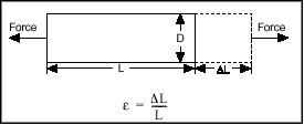
1. Overview  - http://www.ni.com/white-paper/3092/en/Strain is the amount of deformation of a body due to an applied force. More specifically, strain (e) is defined as the fractional change in length, as shown in the figure defining strain gauge below. 


Definition of Strain 

Strain can be positive (tensile) or negative (compressive). Although dimensionless, strain is sometimes expressed in units such as in/in or mm/mm. In practice, the magnitude of measured strain is very small. Therefore, strain is often expressed as microstrain (), which is E x 10-6

When you strain a bar with a uniaxial force, as depicted in the figure defining strain gauge above, a phenomenon known as Poisson strain causes the girth of the bar, D, to contract in the transverse, or perpendicular, direction. The magnitude of this transverse contraction is a material property indicated by its Poisson's ratio. The Poisson's ratio (v) of a material is defined as the negative ratio of the strain in the transverse direction (perpendicular to the force) to the strain in the axial direction (parallel to the force), or . For example, Poisson's ratio for steel ranges from 0.25 to 0.3.

2. The Strain Gauge


While there are several methods of measuring strain, the most common is with a strain gauge. A strain gauge's electrical resistance varies in proportion to the amount of strain placed on it. The most widely used gauge is the bonded metallic strain gauge.
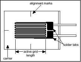
The metallic strain gauge consists of a very fine wire or, more commonly, metallic foil arranged in a grid pattern. The grid pattern maximizes the amount of metallic wire or foil subject to strain in the parallel direction (shown as the "active grid length" in the Bonded Metallic Strain Gauge figure). The cross sectional area of the grid is minimized to reduce the effect of shear strain and Poisson strain.


Bonded Metallic Strain Guage

It is very important that you properly mount the strain gauge onto the test specimen. This ensures the strain accurately transfers from the test specimen through the adhesive and strain gauge backing to the foil. 

A fundamental parameter of the strain gauge is its sensitivity to strain, expressed quantitatively as the gauge factor (GF). Gauge factor is the ratio of fractional change in electrical resistance to the fractional change in length (strain):


The gauge factor for metallic strain gauges is typically around two.

Ideally, the resistance of the strain gauge would change only in response to applied strain. However, strain gauge material, as well as the specimen material to which you apply the gage, will also respond to changes in temperature. Strain gauge manufacturers attempt to minimize sensitivity to temperature by processing the gauge material to compensate for the thermal expansion of the specimen material intended for the gauge. While compensated gauges reduce the thermal sensitivity, they do not remove it completely. For example, consider a gauge compensated for aluminum that has a temperature coefficient of 23 ppm/°C. With a nominal resistance of 1000  GF = 2, the equivalent strain error is still 11.5 /°C. Therefore, additional temperature compensation is important.
See Also: 
How is Temperature Affecting Your Strain Measurement Accuracy?


3. Measuring Strain


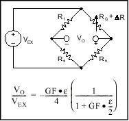
In practice, the strain measurements rarely involve quantities larger than a few millistrain ( x 10-3). Therefore, measuring strain requires accurate measurement of very small changes in resistance. For example, suppose a test specimen undergoes a substantial strain of 500 . A strain gauge with a gauge factor GF = 2 will exhibit a change in electrical resistance of only 2·(500 x 10-6) = 0.1%. For a 120  gauge, this is a change of only 0.12 .


Quarter-Bridge Circut 

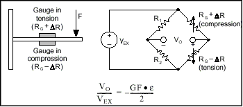
Alternatively, you can double the sensitivity of the bridge to strain by making both gauges active, although in different directions. For example, the Half-Bridge Circuit figure illustrates a bending beam application with one bridge mounted in tension (RG + R) and the other mounted in compression (RG - R). This half-bridge configurati
on, whose circuit diagram is also illustrated in the Half-Bridge Circuit figure, yields an output voltage that is linear and approximately double that of the quarter-bridge circuit.


Half-Bridge Circuit
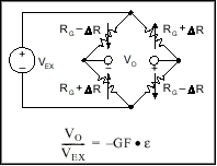
Finally, you can further increase the sensitivity of the circuit by making all four of the arms of the bridge active strain gauges and mounting two gauges in tension and two gauges in compression. The full-bridge circuit is shown in the Full-Bridge Circuit figure below.


Full-Bridge Circuit

The equations given here for the Wheatstone bridge circuits assume an initially balanced bridge that generates zero output when you do not apply strain. In practice however, resistance tolerances and strain induced by gauge application will generate some initial offset voltage. This initial offset voltage is typically handled in two ways. First, you can use a special offset-nulling, or balancing, circuit to adjust the resistance in the bridge to rebalance the bridge to zero output. Alternatively, you can measure the initial unstrained output of the circuit and compensate in software. 

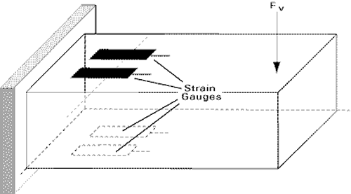
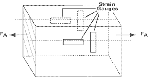
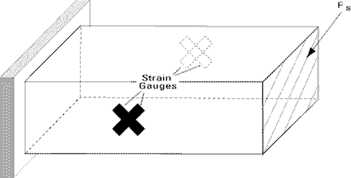
With this in mind, there are several types of commonly measured strain (in order of relative popularity):

Bending Strain -- resulting from a linear force (FV) exerted in the vertical direction.

Axial Strain -- resulting from a linear force (Fa) exerted in the horizontal direction.


Shear Strain -- resulting from a linear force (FS) with components in both the vertical and horizontal direction.

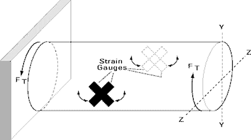
Torsional Strain -- resulting from a circular force (FT) with components in both the vertical and horizontal direction.

4. Choosing the Right Type of Strain Gauge


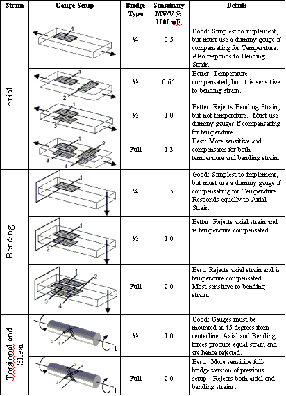
The two primary criteria for selecting the right type of strain gauge are sensitivity and precision. In general, if you use more strain gauges, (a full-bridge circuit rather than a quarter-bridge) your measurement will respond more quickly and be more precise. On the other hand, cost will also play a large part in determining the type of strain gauge you select. Typically, full-bridge strain gauges are significantly more expensive than half-bridge and quarter-bridge gauges. For a summary of the various types of strain and strain gauges, please refer to the Strain Gauge Summary table below.

Strain Gauge Summary